I'm building a beefed-up version of the VESC.
When I measure a low-side gate, I see this:
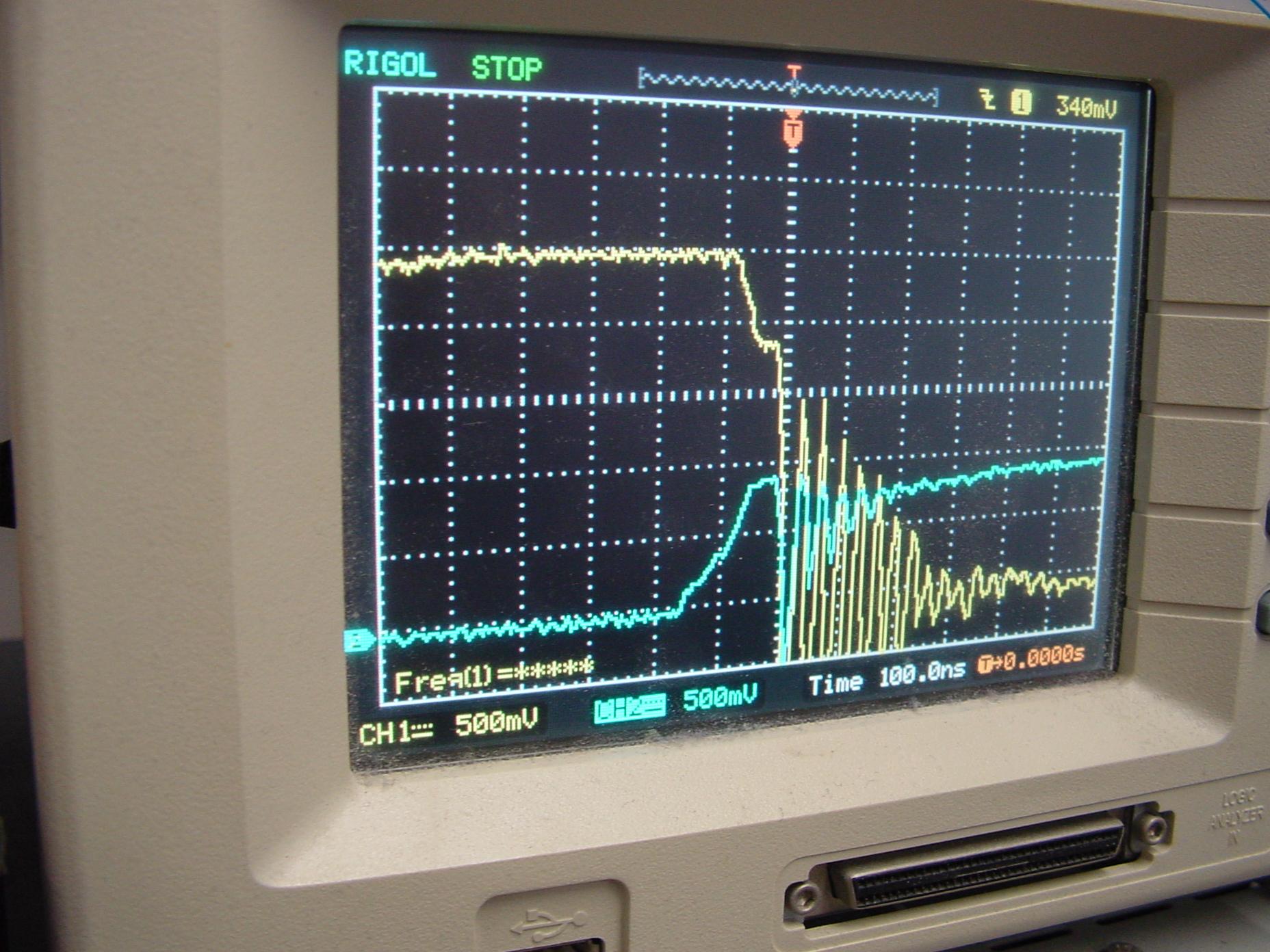
So... When the low-side FET turns on, after a while the turn-on is so fast that through the output capacitance of the FET the gate turns completely off again. Not quite a miller plateau.
This happens almost 3 times in 100ns, so at about 30Mhz. Now I could increase the gate resistance to make the turn-on slower, but this also gives my gate driver less authority to keep the gate at the "wanted" voltage.
My gate driver claims "4A", and I now have 4.7 Ohm gate resistors. So with the gate driver being close to 10V already, with a negative gate voltage we should be seeing > 2A through the gate resistor. Oh. I have two parallel FETs nowadays..... They have separate gate resistors.
The probes are 1:10 so when the scope says 500mV/div it really means 5V/div. As you can see I'm running at 24V right now. (at around trigger-500ns you can see that the highside fet releases this phase so the voltage rises to 24.6V)
First thing to do is to be sure that it's not the scope probes that cause the trouble.
You can solder small 100k resistors to the test points you use and measure with those resistors in series, with 100K and 10:1 probes the measurement error will be low enough.
That will insulate the capacitance and inductance of the probes.
If it doesn't work it may come from the paralleling of the MOSFET.
You can put a small ferrite bead in series with each gate.
Hope this helps.
Have a Nice Day.
Thierry
I'm using the 10:1 setting of the probe because that loads the test point with only 10M. Your suggestion of adding 100k to that is not going to matter much.
The measurement errors are not caused by the load of the probe on the signal, but by the sudden changes in currents that cause resistive and inductive voltage drops where you don't expect them. Also magnetic fields caused by the currents will induce voltages in say the ground clip wire for the probe.
Today I took some further measurements. I see about 4V across the aluminium bar that carries "ground". The cross section of that bar is 3x30mm, so 90 mm^2.
My suggestion of adding 100K resistor was not related to impedance, but in order to insulate and avoid electromagnetic pick-up, especially in the ground clip and wire.
You can also add a resistor (10k for example) from gate to source directly on the pins of the Mosfet because the current will be low (about 1mA) compared to the charging/discharging current, but it will help reducing pick-up "noise".
But I didn't imagine you use such big bus bars :-)
Thor, Lizardmech, or Paltatech will give you more good advices, beacause they also do large current controllers.
Have a Nice Day.
Thierry
I don't see how that can "reduce pickup noise" unless the gate is not being driven. The VESC design calls for a 33 or 39k resistor to ground for that situation. Even though my design uses a FET driver that should always be driving the gate, I have kept that resistor.
What I think happens is that when the mosfet starts to conduct, the drain node is yanked from "V+" to GND so quickly that capacitive coupling between that node and V+ causes the ground in the rest of the system to be yanked down as well. The gate driver is driving the gate at "V-GROUND+8V at that point in time and that ends up being yanked down as well.
All this is difficult to measure as simply hooking up a ground clip to "the ground" is not giving you ground potential.
Due to the skin depth effect, that 90 mm2 conductor is only .9mm2 at 33MHz. I didn't realize that until now.
To carry my half-bridge module through power surges lasting on the order of 30ns with a voltage loss less than 1.5V, I would need C = I dt/dU = 100A . 30ns / 1.5V = 2uF. I have that.
Yes, a friend has a similar problem and will use "Litz wire" composed of more than 10x 0.8mm enamelled wires.
Have a Nice Day.
Thierry
I did some more thinking/measuring. It's not the ground bounce. I have now artificially increased the gate capacitance and that dampens the effect enormously. I now have a half-decent miller plateau.
What does the pcb layout look like? One option is ferrite beads in addition to the gate resistors, they offer high resistance in the mhz range while letting lower khz range through.
Yes, I suggest this (ferrite bead) on my first answer.
You can find 50 ohms to a few k values, the best is to find the right one with some trials.
The PCB layout is also very important.
Have a Nice Day.
Thierry
The ferrite bead, IMHO won't work. The 40mm trace from the driver chip to the gate is already too much (about 15nH IIRC). Adding even more . will not help.
The problem is that when the drain starts moving, it couples into the gate, normally creating a miller plateau. But due to "bad wiring" on my end the gate is pushed back past the threshold voltage. So the drain goes back up etc etc. This is now reduced to almost nothing by adding a bit extra capacitance. If possible I'll add a discharge-bypass-diode on the resistor on the next revision of the PCB.
Now things seem to survive current settings of 100A + . I'm happy!
Because I only have a 2 channel scope, and it has limited sample-depth I have decided to grab all the gate drive signals and halll sensor signals with my logic analyser.
I have written a decoder program that analyses the LA dumpfile, and outputs the hall states as 6 numbers from 0 - 1.
I have written a decoder program that analyses the LA dumpfile and outputs the PWM number as a floating point percentage.
This is a clean startup at 30A motor current. At the right the 95% dutycycle was reached. You can also see why I wanted 0-1 numbers for the hall sensor state: Now I don't have to figure out how to get separate scales in gnuplot.
But with 100A the startup looks a whole lot different:
All of a sudden there are many regions with out-of-character PWM values. I've considered "measurement error" or "decoding error", but things look "too neat" for that.
When I measure say one such red-blue band near the right, and scroll to the area in the logic analyser program, I see periods of about 7 PWM cycles with one PWM setting and then a wild change for another 7 PWM cycles, going for example from 12% to 97% without anything inbetween.
In the case at hand, the A and B PWM values keep alternating between say 10-90 and 90-10, while C stays close to 50%.
Any suggestions what this could be?
OK, I better understand the problem now.
You have to dampen a lot, not an easy task, and difficult for me without being near the set-up.
Try local bypass capacitor, preferably special film capacitor like MKP designed for high dv/dt and di/dt.
Also try snubber and rc filter between drain and gate, and gate and source.
Some zener can also help to clamp.
Have a Nice Day.
Thierry
Hi, I got same problem. Did you find solution to this?
I soldered a 22nF capacitor between gate and source.
can you share layout? it can be large inductance between source and capacitors or gate resistor is not close to gate or parasitic capacitance between gate and drain(like added by layout)
Well. with currents above 100A and voltages of 200V I HAVE to space things out. The IRFP4668 by itself is not enough. I have two of them in parallel for each leg.
I have listened to the power guys and placed the ground rail as close as possible to the power rail. I've used plenty of metal (90 mm^2) for that.
Anway, in the end you get to hear: "Oh, but your gate traces are way too long". We'll I've done all I can to make things as compact and close together as I can. But I need 8mm screw terminals to carry the current etc etc.
All in all, it seems to work now. I've "slowed" things down, so I'm not as efficient as it could be. But I am not going to need the 100A for long. So when after a few seconds the current drops say by 50%, efficiency and heat arguments are suddenly a factor of 4 less relevant.... So far I seem to be able to run at 100A for a coulple of minutes, but things like batteries then tend to start heating up. All in all... for me the current situation is fine. I'll optimize trying to get rid of the extra caps later....
That's not uncommon.
Most Chinese e-bike controllers (Kuteng, BMS battery S06S,..) have 10nF between gate and source.
Sure you'll succeed improving your layout and decrease the cap value.
Have a Nice Day.
Thierry
But isn't that going to also slow down the FET switching speed - causing larger switching losses which means more heat ..?
(unless you don't care about heat as much as actually fixing the problem that Roger is facing of course..)
Yes, slowing down the switching is not helping the switching losses. But the ringing is way worse: It causes many switches from on to off and back when only one was commanded.