Hi all,
i have a problem with my custom PCB and higher currents. I think it is a hardware bug. With higher currents, the battery current, battery voltage and motor current have high ripple. Very often the curent out of sync error is reportet. but not allways
i guess there are too less caps near to the FETs and maybe i need a "global" cap at the battery input. Can someone confirm this ? or is this a more a software problem ?
schematic is found here https://github.com/CTSchorsch/gsvesc/blob/master/pdf/gsvesc.pdf
Regards
Georg
It would help to see a picture of the populated PCB, with higher power ESCs the PCB layout is extremely important.
Hi TheFallen,
thanks for your reply. If you have KiCad you can open the projekt from the git repo. If not here is a picture and a pdf print of each layer
Thanks
Georg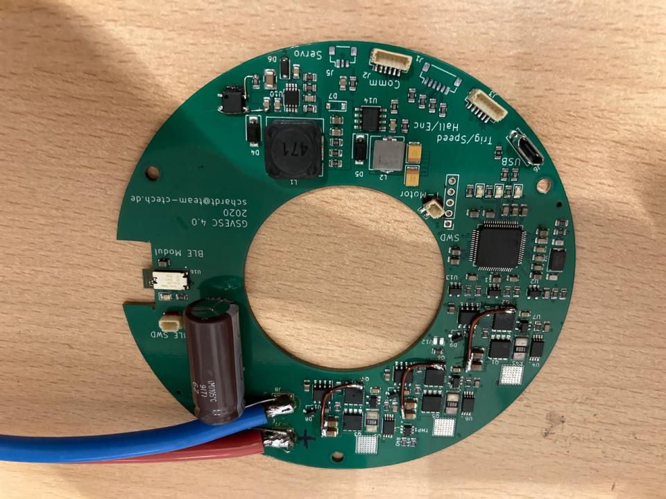
gsvesc-F.Cu_.pdf
gsvesc-In1.Cu_.pdf
gsvesc-In2.Cu_.pdf
gsvesc-B.Cu_.pdf
I would love to know why your local decouplers have a giant mod wire?
I think your problem is having the current amps right next to the power sections. Run your differential traces back and put the amps right next to the MCU. The single ended output of the amps is very sensitive to noise compared to the differential voltage across the shunt.
For the vsense I can't tell where the voltage divider is, but also want to put the divider and filtering as close to the MCU as you can.
Hi TechAUmNu,
nice wires, or ? :)) I forgot some vias to connect the local FETs to the inner ground plane. This makes the path from FET-GND to CAP-GND very long... i want a good connection :)
Okay, until now, i thought that the signal after the amp is much more stable than the differential lines with lower signal. Are you sure to route the tracks from the shunt the long way to the mcu ?
The voltage devider are between power part and mcu, three in a row :) is this a good placement ?
- Do I need more local caps ? there are two 10u 75V placed per phase
- Do you think i have to split grounds between power and digial/analog ?
Thanks for your feedback
GEorg
I think you want to reduce the loop length for the local caps. The bigger the area the form to join Vsupply and ground the more noise you will have.
Never done a split ground on my boards, don't really see its going to make that much diffence unless you are running supply currents in the ground plane past sensitive parts.
The voltage dividers are fine there.
Yes for the current sense differential traces routed properly should be able to go quite a long way without any detrimental noise as the amplifier will remove any common mode noise that appears. But a thin highish impedance single ended signal from the amplifier that only varies by a few mv will be very sensitive.
Thx TechAUmNu,
i will try to realize all your (and some other) input in the next redesign.
but once again, the current sense amplifier: i have a 1 mOhm Shunt, so only around 50mV signal on the differential lines. Is this fine for the amplifier ? i can not belive that 50mV signal with much more noise can be removed by the amplifier.
The current sense is differential from the shunt, so you have 2 parallel conductors. They are close together, so see almost identical interference (common mode noise). When you then subtract one signal from the other you will only see the difference between them, so the common signal on both of the conductors caused by the interference will be removed.
For the single ended signal going along the same path, you have no way to remove this common noise as there is no reference.
Thanks again. I will try :)
Hi TechAUmNu,
i did a small redesign. I tried to separate the Power-Part from all the other stuff. I added some caps to the power input and move the local phase Cs near to the FETs. Amps and Driver a move away from power.
Power is routed on two layer with one exception: Phase current is only on one layer because vias would destroy the inner planes. do you think this is okay for the short way ?
Here are the gerber prints:
gsvesc-B.Cu__0.pdf
gsvesc-F.Cu__0.pdf
gsvesc-In1.Cu__0.pdf
gsvesc-In2.Cu__0.pdf
Thanks
Georg
Sooo much better :D
I think your phase tracks from the top fet there might fuse, I would move the shunt so it connects in the middle between the two fets (ie put the shunt at the thin bit). Then you have much shorter track.
If those are 10uF caps you can get away with only 2 and have more room for phase track.
Thanks :)
i have problems to move the Phase C shunt, because the vias of the Motor Pad cuts the planes on layer 3&4. i will try :)))
Georg
I move the shunt in the middle. Looks better. Do you think the bottom plane is big engough for Vbat ? The same plane is on layer 3
That looks better, that plane is probably fine. You can use Saturn PCB to work out track widths: http://saturnpcb.com/pcb_toolkit/
Thanks again for your help.
Unfortunately some parts are out of stock at jlcpcb :( i have to wait with my pcb and assembly order
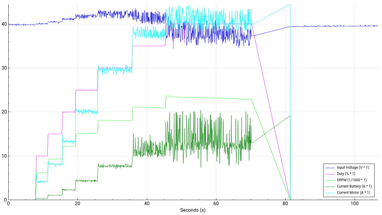
ready to test :) now smoke signals, firmware uploaded
Looking good :D
One thing I might do is move your NTC for the mosfet temperature to right next to one of the fets, then put some copper under the NTC connected to the fet, will give you a much better measure of the actual temperature.
mmh, to use copper is a nice idea. i use capton tape on the fet and glue the ntc on the capton tape... works also very good
Here two pictures of the current measurement, just before the adc. First the old pcb:
and with the new pcb
i don't now which influence the base noise has, but the big spikes are eliminated. Pictures were taken with 6A phase current