Hi,
I have been reading about protecting mosfets for 100V designs - and I am a bit confused,
different app notes have different suggestions and I am not sure as to the purpose for all of them,
I am looking to create a high reliability design - the one that should not fail, what are the protection mechanisms that I can put in place? - essentially asking how to design the power stage.
Here is what I have so far:
1. On the input side, make sure there is no shoot through condition by High and Low side switching on at the same time - can use logic gates like Axiom
2. Pull down resistor (10K) from gate to source
3. Tidrinhv2 guide has this setup - TVS diodes gate to source ; separate discharge path using schottky for gate
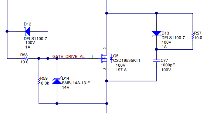
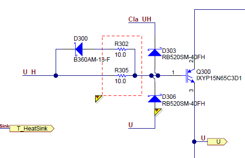
4. tidrin2 has this setup: schottky diodes from source to gate and gate to drain
5. Optimize gate resistor ?
so that there is little overlap between the high side and the low side as well as no ringing at mosfet gate
6. Place gate resistors next to the mosfet gate
7. Gate driver selection - mosfet gate charge should be filled in 0.1% of the PWM frequency time period ?
8. trace length from gate driver to mosfets should be minimum
9. Simple RC filter for PWM input into the gate driver
10. Current limiting resistor for power to the gate driver - how to select ? any recommendations ?
11. Fast schottky diode for bootstrap diode power - how to select ? any recommendations ?
What else should I be looking out for ?
and which protection to use (3) or (4) ?