Hi Folks,
Like many here I am working on my own VESC derivative that I am tentatively calling the TINY6. I based my hardware off of the VESC 6.4 and antonchromjak's MINI4 (and learned a lot from others, thank you everyone for open source designs!). I'm about ready to send my design off to be manufactured but before I do, I figured wouldn't hurt to see if anyone wanted to sanity check some of my design decisions.
My application is for ~2810 bldc motors running on 4S and pulling ~3A continuous. For safety, I designed the board for a max of 25V, 10A continuous, 30A peaks. Eventually I will integrate two of these into a board with some other stuff on it. It is important I keep the footprint as small as possible.
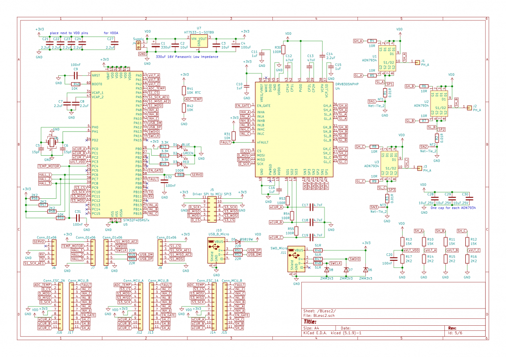
For the MOSFETs and gate driver, I chose to use three AON7934 Dual N-Channel MOSFETs and the DRV8305N. The DRV8305N is nice because of the included current-shunt amplifiers and has configurable settings with SPI. Among other settings, I plan to disable several of the fault conditions and up the gate driver peak sink and source currents over SPI. A downside is they can't be used for inline sensing, but from what I have read 3 phase low-side sensing is not too much worse and the board space is worth it to me.
My Shunt resistors are 10mΩ 1206 1W. At 30A peaks, the differential input voltage will be 30A*10mΩ = 0.3V, safely under the 0.48V max for my amps. At 10A continuous, the resistors will dissipate 10mΩ * 10A^2 = 1W. Between 0A and 3A continuous, the amplifier will output between 3.3V/2 = 1.65V and 3.3V/2 + 3A*10mΩ*20V/V = 2.25V, giving me a range of 0.6V. If I find I'm really only using up to 3A and am wasting too much of my ADC range on FoS, I can up the amplifier gains over SPI.
My voltage dividers can handle 25V. 25V*2.2K / (15K + 2.2K) = ~3.2V.
To limit my gate sink and source current to under 1A I included 10Ω gate resistors (planning for ~2Ω MOSFET gate resistance). 10V/(10Ω + 2Ω) = 0.83A. Dead time is my biggest fear for my design right now. I know it can be adjusted in the vesc firmware and in the DRV8305 over SPI, but I still need to figure out what to set mine to.
For bulk capacitance, I included a 10uF capacitor by each half-bridge and a 330uF low esr capacitor for the board.
About the prototype schematic and board design:
I have anything I could want on the prototype but will experiment with removing elements I don't need. All the passive filters (current, servo, motor temp) were pulled right from the 6.4 design and I want to experiment with removing them. The ADC_TEMP resistors are also on the chopping block. For the final design I will move from mostly 0603 passives to 0402s. The SPI bus for the DRV8305N can be jumped to the STM32s third SPI bus or an external SPI bus.
A few style things I am sorry for in advance:
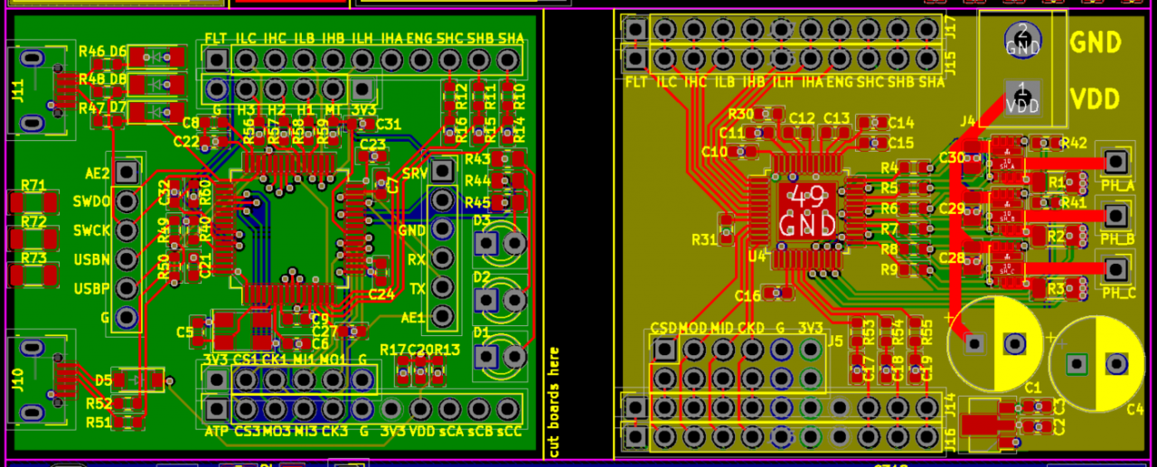
- Unlike the final design, the prototype is broken into a control board and a power board. This will help with testing/debugging, and will eventually help me test alternative stm32s (considering the STM32F411CEU6?). The way I separated the circuits in the schematic is terrible and leads to unhappy ratlines, but I'm too lazy to do it right when the final won't have this.
- The SWD micro-usb port. I have designed several of my stm32 boards to be programed over SWD using a micro-usb adapter I made for my st-link v2. It's perhaps awful style but it is compact, quick, and robust compared to pin headers.
When my boards get here I will run the following tests:
- First I will test uploading default 6.4 firmware over SWD to the control board and confirm I can connect with it over USB using vesc tool
- Then I will compile and upload firmware using HW_60.
- Next I will create a new hw config to match my hardware based off of HW_60, then compile and upload that.
- Then I will modify the DRV8305N settings. I will do this with a separate microcontroller and will have to redo the changes every time I power cycle.
- Only after everything looks good will I put the control board and power board together and do a full system test.
- Hopefully I will be able to spin a test motor and can start dialing stuff in.
- eventually I want to make the stm32f405 change the DRV settings on startup.
Any suggestions would be appreciated. I will post updates and eventually the final design as development continues.
Cool!