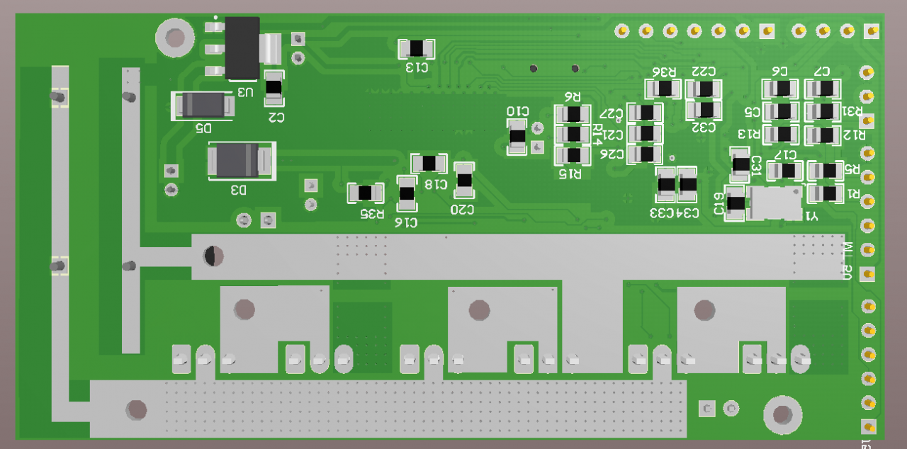
 Bottom
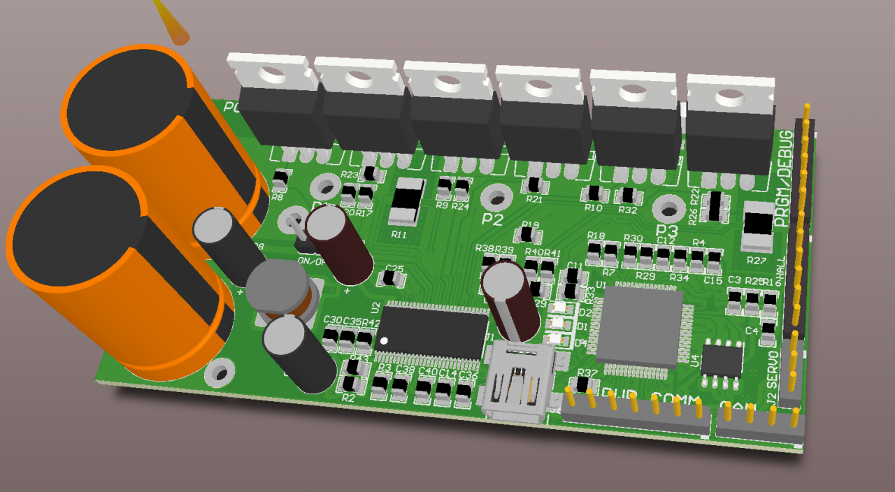
TOP
Hey there. I’m rehashing the VESC into a cheaper 2 layer version with external FETs. I’ll call it the Cheap VESC for now. You may notice it resembles the generic ebike controllers that you can find on ebay/aliexpress. This is a version that would probably cater more toward the ebike/e-scooter community but probably could still fit just fine on a skateboard. The primary goal here was to make a version of the VESC that is cheaper to create by reducing the original design to 2 layers (check out JLC PCB for super-duper cheap 2 layer boards) and reduce BOM cost a little. The secondary goal was simply to improve my PCB layout and design skills. I still haven’t finalized the design but I would say I am at least 95% done with only a few minor problems to tidy up. If after reading all of this anyone has any suggested improvements to the current or future designs, please feel free to respectfully make them in this thread. Note that this is my most complex board design for me so far with my previous experience being only with simple audio effect boards and circuits.
Cheap VESC
Advantages
- Lower build and BOM cost
- TO-220 FETs allow for big heat sink attachment for excellent thermal performance
- SMD components no smaller than 0805 make hand assembly practical
- Added ON/OFF capability to turn off control circuitry when controller is not in use. A simple mechanical switch will achieve this when connected to the “ON/OFF” 2-pin header.
Disadvantages
- Larger than original VESC. Cheap VESC is 45mm x 92mm
- Higher profile with TO-220 package FETs
- Additional assembly steps to beef up high-current traces. 2 layers of 1oz copper can’t handle the current flowing through during operation. Assembler will have to apply wire/solder wick/bus bar to the exposed Power, Ground, and Phase traces that you can see in the “bottom” image.
Potential features of Future Versions
- Implementing DRV8353 for higher voltage operation (I estimate at least 20s capable). Will need stable version of VESC 6 firmware/software for the 3 phase current sensing and stuff.
- On-board circuitry for no-spark connection
- On-board Bluetooth capability for interface with Open Source Android app for the VESC
- I may create a 12 MOSFET version with the FETs in parallel for even greater power.
Notes
- I intend to test the design rather thoroughly after I get a version assembled. I intend to power a motor under load with different loads while observing temperature with a thermal camera. I will test other features of the design to ensure quality. Because of all this, it will be some time before I release the design files. I don’t want to give the community a broken thing.
If you want, I can help you design a schematic that would make this design non-reliant on the DRV83XX driver to cut costs and enable 100v compatibility? It would add parts but mean the same board could be used for both 50v applications and up to 100v~ applications. There are some other benefits too, like the 60V board would be much more rugged (because some components would be rated much more highly), the components would be easier to solder (no components with thermal pads like that DRV83XX) and more scalable (discrete gate drivers)
@bgdwiepp
I don't mind straying away from the DRV83XX as long as the VESC firmware/software can still be compatible. I would probably look to do your suggested approach in a 12 FET design for higher power applications and the board will already be inherently bigger because of that. I'm still looking to keep the 6 FET version as small as possible though. I really appreciate your offer to help me out I am open to whatever you bring to the table.
Ok, cool.
I think there is quite a bit I can offer, I'd like to know a few little things first though before I start making suggestions;
The position of the MOSFETs, is this fixed? I think you're placing them there so they line up with the aluminum mount on the existing 6 fet e-bike controller cases correct?
What kind of priority do you have on cheap vs small vs performance?
For space reasons, I assume you are going to have direct wire-board connections for input signals, or would you use connectors?
(If you use connectors I highly suggest you do not use 0.1" headers.)
How much do you value ease of assembly?
(I noticed you have components on both the top and bottom)
How strong is your preference for a 2L design?
(2L PCBs from JLC are quite cheap, but 4L boards of this size from JLC aren't expensive either, especially if you include postage costs, and if you are building more than a single unit).
What EDA package do you use, and would you be willing to share design files?
Cool, that seems pretty clear then.
I think you should aim to move all the components to the top layer, this will greatly help hand assembly, as you can paste and reflow all at once, allowing the use of only a single stencil if desired by the builder. Also it allows people to use a skillet to reflow the board if they wish, as the board should sit flat.
One of the ways to help achieve this is to use the narrow/high density SMD footprints for components - this makes them slightly more difficult to solder with a iron, but doesn't effecf other reflow methods.
I was going to suggest direct wire to board rather than 0.1", or JST-XH (I think that's what the original VESC uses), if you use a connector it makes it difficult to use the grommet/seal that some of these cases come with, leading to potential weather proofing issues.
Yeah, that is about the price difference I am seeing; on a single unit the price difference is pretty significant, from 65 as a 2L to 95 on 4L.
I think with careful design this controller should have little issue operating 72V, 50A continuous. One of the main issues for power handling on the VESC is heat dissipation - with the 6 FET design you use the case as a heatsink and suddenly heat dissipation capabilities increase massively.
I use Altium Designer and Cadence Allegro, so that is no issue for me, I immediately recognised the Altium 3D view but wanted to confirm.
I think in this case, using LCSC as the component distributor makes sense as they offer free shipping with JLCPCB and they offer quite a few very nice parts that are unavailable through mouser/digikey/Darnell etc.
I would absolutely have to go with smaller SMD components to fit everything on one side while keeping the board to same dimensions. My concern is that 0603 would be too difficult to handle by the average DIYer, but maybe my concerns are misplaced. A single sided board would definitely make reflow easier. Do you think 0603 size components are within DIY capability for those capable of basic reflow soldering?
Redesigning this to one sided will most likely be implemented on a future version in KiCad. For now, I'll deal with the difficulty of this double sided board design and keep an updated Github repository for all of the designs to come. Note that I haven't made the github repository yet.
Using the case as a heatsink has been the goal already. I'm just unsure of what currents I can get away with when doing that. I intend to test the controller in lab with varying loads while taking temperature readings with a FLIR thermal camera. I'll see how big of currents this thing can handle by direct measurement. Also for this design I'm limited to about 50V operation with an absolute maximum of 60V due to the DRV8302.
I've seen LCSC and browsed their inventory. They have super cheap IC's but they make you by a minimum of 50pcs for the passives I need. They also don't have the current sense resistors I need. I will to split my BOM order between LCSC and another distributor while buying what I can from LCSC. I also intend on using tayda electronics for the passives as they are super cheap for low quantity orders.
Also I think you deserve to know I have a similar thread going on in endless sphere here. It's a larger forum and I wanted input from a large sample. I certainly don't mind continuing our conversation here along with anyone else that wants to join in.